Study on properties of Ti films prepared by magnetron sputtering and electron beam evaporation
-
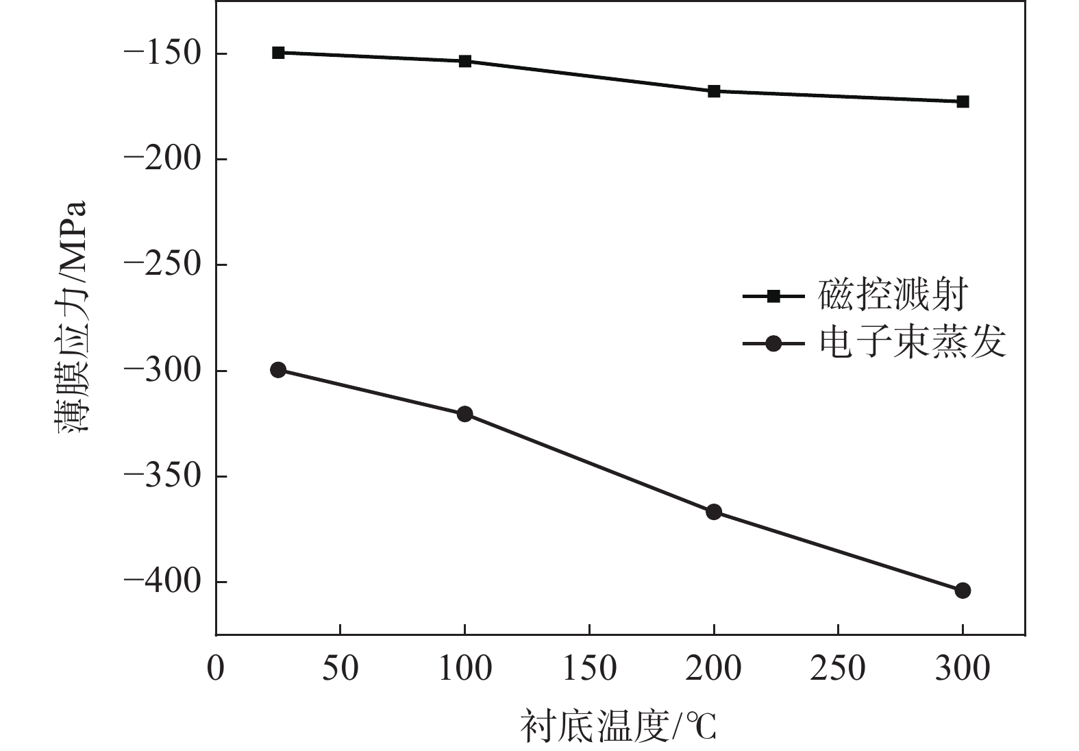
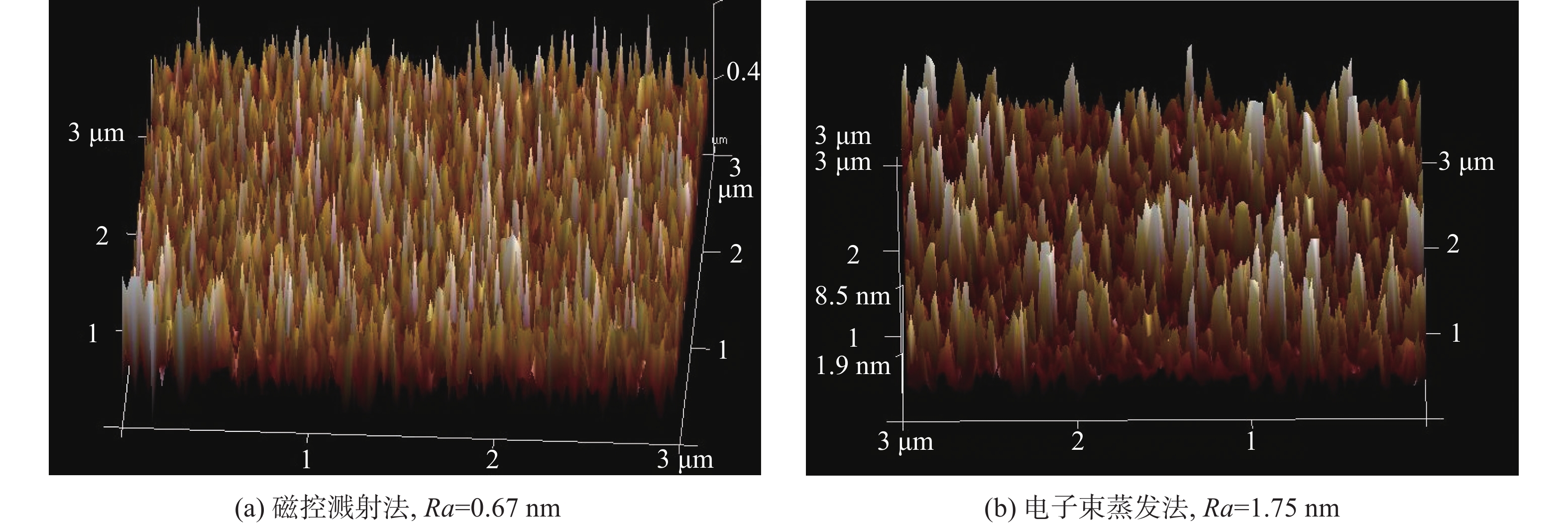
摘要: 为了研究不同制备方法对薄膜性能的影响,分别利用磁控溅射法和电子束蒸发法在长有500 nm厚的SiO2薄膜的Si(100)晶圆上制备了生长速度为1.0 nm/s,厚度为100 nm的Ti薄膜,并对薄膜的厚度、表面形貌、电阻、反射率及应力进行了测试。相比于电子束蒸发法,磁控溅射法制备的薄膜表面晶粒更加均匀致密,表面缺陷少,粗糙度较小,薄膜具有更低的电阻、应力以及更高的反射率。试验结果表明,磁控溅射法制备的薄膜电性能优于电子束蒸发法。电子束蒸发法制备的薄膜应力具有较大的变化范围,可用于多层膜之间的应力匹配调试。同时,也可以通过减少薄膜表面结构缺陷,减小薄膜表面粗糙度来提高薄膜的性能。Abstract: Aiming at studying the effects of different preparation methods on the properties, Ti films with a growth rate of 1.0 nm/s and a thickness of 100 nm were prepared on Si(100) wafers with 500 nm thick SiO2 films by magnetron sputtering and electron beam evaporation methods respectively. The thickness, surface morphology, resistance, reflectance and stress of Ti films were measured. Compared with electron beam evaporation, Ti films prepared by magnetron sputtering have a more uniform and denser surface with fewer defects and smaller roughness, lower resistance, stress and higher reflectance. The results show that the electrical performance of Ti films prepared by magnetron sputtering are superior to that of electron beam evaporation. The stress of Ti films prepared by electron beam evaporation has a large range of variation, which can be used for the stress matching debugging between multilayer films. The performance of the films can be improved by reducing the surface structural defects and surface roughness.
-
Key words:
- Ti films /
- magnetron sputtering /
- electron beam evaporation /
- resistance /
- reflectance /
- stress
-

图 1 25 ℃下磁控溅射法(a)和电子束蒸发法(b)制备的Ti薄膜表面的AFM形貌
Figure 1. AFM morphologies of Ti films prepared by magnetron sputtering(a) and electron beam evaporation(b) at 25 ℃

图 2 不同温度下磁控溅射法和电子束蒸发法制备的Ti薄膜的残余应力
Figure 2. Residual stress of Ti films prepared by magnetron sputtering and electron beam evaporation at different temperatures
表 1 25 ℃下磁控溅射法和电子束蒸发法制备的Ti薄膜性能比较
Table 1. Properties of Ti films prepared by magnetron sputtering and electron beam evaporation at 25 ℃
制备方法 电阻/Ω 电阻均匀性U/% 反射率/% 磁控溅射法 7.2 0.92 55.4 电子束蒸发法 8.1 2.24 53.4  下载: 导出CSV
-
[1] Zhang L, Shi L Q, He Z J, et al. Deposition of dense and smooth Ti films using ECR plasma-assisted magnetron sputtering[J]. Surface and Coatings Technology, 2009,203(22):3356−3360. doi: 10.1016/j.surfcoat.2009.04.022 [2] Jin Y, Wu W, Li L, et al. Effect of sputtering power on surface topography of dc magnetron sputtered Ti thin films observed by AFM[J]. Applied Surface Science, 2009,25(8):4673−4679. [3] Jeyachandran Y L, Karunagaran B, Narayandass S K, et al. Properties of titanium thin films deposited by dc magnetron sputtering[J]. Materials Science and Engineering A, 2006,431(1/2):277−284. [4] Savaloni H, Faridshayegan F. Film thickness dependence on the optical properties of sputtered and UHV deposited Ti thin films[J]. Vacuum, 2010,85(3):458−465. doi: 10.1016/j.vacuum.2010.08.023 [5] Wang Hong, Wang Jinshu, Li Chun, et al. Effects of deposition parameters on microstructure of magnetron sputtered Ti films and the following anodization[J]. Journal of Beijing University of Technology, 2013,(2):263−268. (王鸿, 王金淑, 李春, 等. 磁控溅射参数对钛薄膜结构及阳极氧化的影响[J]. 北京工业大学学报, 2013,(2):263−268. [6] Cai Changlong, Liu Jingwei, Wu Shenjiang. The preparation technology and physical characteristics research of titanium films[J]. Initiators & Pyrotechnics, 2015,(4):17−20. (蔡长龙, 刘经纬, 吴慎将. 钛薄膜制备工艺及物理特性研究[J]. 火工品, 2015,(4):17−20. [7] Wu Yangwei, Zheng Mingzhi, Lin Limei, et al. Structural and optical properties of titanium films prepared by magnetron sputtering[J]. Journal of Fujian Normal University(Natural Science Edition), 2012,28(4):31−35. (吴杨微, 郑明志, 林丽梅, 等. 磁控溅射制备钛薄膜的结构和光学性质[J]. 福建师范大学学报(自然科学版), 2012,28(4):31−35. [8] Cai K, Muller M, Bossert J, et al. Surface structure and composition of flat titanium thin films as a function of film thickness and evaporation rate[J]. Applied Surface Science, 2005,250(1-4):252−267. doi: 10.1016/j.apsusc.2005.01.013 [9] Zou Penghui, Huang Nianning, Wang Yanshuo, et al. The effect of evaporation rate on the Ti/GaAs schottky barrier[J]. Research & Progress of SSE, 2015,35(5):502−505, 511. (邹鹏辉, 黄念宁, 王彦硕, 等. 电子束蒸发速率对Ti/GaAs肖特基势垒特性的影响[J]. 固体电子学研究与进展, 2015,35(5):502−505, 511. [10] Arshi N, Junqing L U, Chan G L, et al. Thickness effect on properties of titanium film deposited by d.c. magnetron sputtering and electron beam evaporation techniques[J]. Bulletin of Materials Science, 2013,36(5):807−812. doi: 10.1007/s12034-013-0552-2 [11] Yu Fengbin, Xia Xianghua, Zhu Deming, et al. Study on performance of Al/PI films prepared by electron beam evaporation and magnetron sputtering[J]. Materials China, 2008,27(6):21−24. (余凤斌, 夏祥华, 朱德明, 等. 电子束蒸发与磁控溅射制备Al/PI复合薄膜的性能研究[J]. 中国材料进展, 2008,27(6):21−24. [12] Li Changwei, Zhang Chujing, Kong Lingqi. Effect of resistance thermal evaporation and magnetron sputtering deposition on two-dimensional Ag nanoparticle array structure[J]. New Chemical Materials, 2014,42(8):67−69. (李昌伟, 张春婧, 孔令琦. 电阻热蒸发与磁控溅射对制备二维银纳米阵列的影响[J]. 化工新型材料, 2014,42(8):67−69. [13] Gao Li, Zhang Jianmin. Comparisons between ZnO thin films fabricated by RF-magnetron sputtering and electron-beam evaporation[J]. Journal of Shaanxi Normal University(Natural Science Edition), 2009,37(3):23−27. (高立, 张建民. 射频磁控溅射和电子束蒸发制备ZnO薄膜特性的比较[J]. 陕西师范大学学报:自然科学版, 2009,37(3):23−27. [14] Li Kun, Xiong Yuqing, Wang Hu, et al. Effect of evaporation rate on the properties of ZnS films[J]. Vacuum, 2021,58(2):15−19. (李坤, 熊玉卿, 王虎, 等. 蒸发速率对ZnS薄膜性能的影响[J]. 真空, 2021,58(2):15−19. doi: 10.13385/j.cnki.vacuum.2021.02.04 [15] Palasantzas G. Influence of anomalous roughness growth on the electrical conductivity of thin films[J]. Physical Review B, 2005,71(20):205320.1−205320.5. [16] Zhao Yiran, Chen Junfang, Shao Shiyun, et al. Electrical property of TiN film deposited by electron beam evaporation[J]. Semiconductor Optoelectronics, 2012,33(1):90−93. (赵益冉, 陈俊芳, 邵士运, 等. 电子束蒸发沉积TiN薄膜的电学特性研究[J]. 半导体光电, 2012,33(1):90−93. doi: 10.16818/j.issn1001-5868.2012.01.022 [17] Liu Yingguang, Han Xiao, Hao Jiangshuai. Effect of grain boundary geometry on the thermal conduction of nanocrystalline ZnO[J]. Rare Metal Materials and Engineering, 2021,50(3):924−931. (刘英光, 韩笑, 郝将帅. 晶界几何结构对纳晶ZnO材料导热过程的影响[J]. 稀有金属材料与工程, 2021,50(3):924−931. [18] Zhu Jingtao, Yue Shuaipeng, Tu Yuchun, et al. Preparation of Co/Ti multilayer in soft X-ray region by nitrogen reactive sputtering[J]. Optics and Precision Engineering, 2015,23(1):10−14. (朱京涛, 岳帅鹏, 涂昱淳, 等. 氮气反应溅射制备软X射线Co/Ti多层膜[J]. 光学精密工程, 2015,23(1):10−14. doi: 10.3788/OPE.20152301.0010 [19] Yu Yiting, Fan Weizheng, Qiao Dayong. Application of curvature measurement technique for measuring residual stresses in MEMS thin film[J]. Chinese Journal of Mechanical Engineering, 2007,43(3):78−81. (虞益挺, 苑伟政, 乔大勇. 曲率测量技术在微机电系统薄膜残余应力测量中的应用[J]. 机械工程学报, 2007,43(3):78−81. doi: 10.3901/JME.2007.03.078 [20] Li Zhaoying, Gong Yansheng, Tian Yongshang, et al. Effect of deposition temperature on structure and surface morphology of TiN thin films prepared by radio frequency magnetron sputtering[J]. Electroplating & Finishing, 2013,32(12):39−41. (李兆营, 公衍生, 田永尚, 等. 沉积温度对射频磁控溅射 TiN 薄膜结构和表面形貌的影响[J]. 电镀与涂饰, 2013,32(12):39−41. doi: 10.3969/j.issn.1004-227X.2013.12.010 [21] Zhao Hengli, Yang Peizhi, Li Sai. Effects of deposition temperature on structures and properties of HfO2 thin films prepared by ALD[J]. Semiconductor Technology, 2022,47(3):205−210, 242. (赵恒利, 杨培志, 李赛. 沉积温度对ALD制备HfO2薄膜结构和性能的影响[J]. 半导体技术, 2022,47(3):205−210, 242. -

 点击查看大图
计量
- 文章访问数: 288
- HTML全文浏览量: 744
- PDF下载量: 102
- 被引次数: 0